IGBT new cleaning solution: dual solvent cleaning, deep cleaning, green and environmentally friendly
IGBT new cleaning solution: dual solvent cleaning, deep cleaning, green and environmentally friendly
In the fields of new energy vehicles, photovoltaic inverters, industrial transmissions, etc,IGBTAs the core power device, the long-term reliability of modules directly determines the safety and lifespan of terminal equipment.SMTThe cleaning of residual flux in the process isIGBTThe key process of packaging —— Failure to meet cleaning standards can pose significant risks such as short circuits, overheating, and failure; However, traditional cleaning methods have always been “Cleanliness, environmental friendliness, compatibility, cost” Difficult to balance, becomingIGBTThe core bottleneck of mass production.Dual solvent cleaning solution - using “Double solvent deep dissolution + Single solvent rinsing + Volatile condensation recovery” The synergistic mechanism improves cleanliness while achieving the recycling and reuse of volatile solvents, greatly reducing solvent loss.
The traditional single solvent cleaning solution requires rinsing with clean water, which generates a large amount of wastewater during the rinsing process. Subsequent wastewater treatment has always been a major challenge for production enterprises, and the high cost of wastewater treatment greatly increases their production costs.The new dual solvent cleaning solution uses volatile solvents for rinsing, and after rinsing, it naturally evaporates and dries. All volatile solvents are refluxed and filtered through a condensing device, which can be recycled. The cleaning process does not produce wastewater, solving the problem of wastewater treatment in traditional single solvent cleaning.
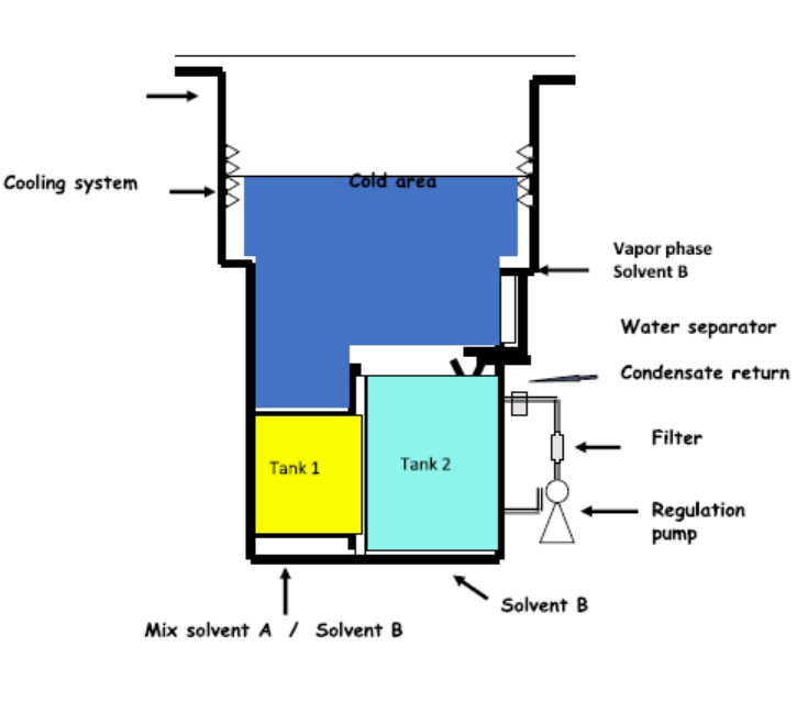
Advantages of dual solvent cleaning solution:
1、 Compatible with the vast majority of materials
2、 Specially designed for stubborn pollutants (suitable for high difficulty cleaning scenarios)
3、 For low standing distance / Low gap components exhibit excellent cleaning performance
4、 Fast drying speed, no residue after cleaning
5、 There is no risk of secondary oxidation during the drying process
6、 No ozone depletion potential (none)ODP)No Global Warming Potential (N/A)GWP), and non flammable
7、 The equipment occupies a smaller area
8、 No wastewater discharge issues
9、 Nitrogen free(N)And phosphorus(P)Elements
10、 Excellent wetting ability (low surface tension), andKBHigh value (strong solubility)
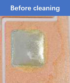
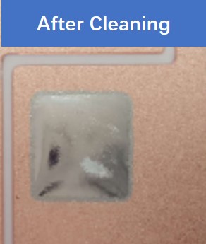
At present,The dual solvent cleaning solution has been widely applied in the semiconductor industry. For more case sharing, please contact Shanghai Mingchengjin Material Technology Co., Ltd